Manufacturing Data Preparation

NPI Suite

Complete CAD/CAM data preparation for PCB manufacturing. From BOM import to production handover, prepare all your manufacturing data in one platform.

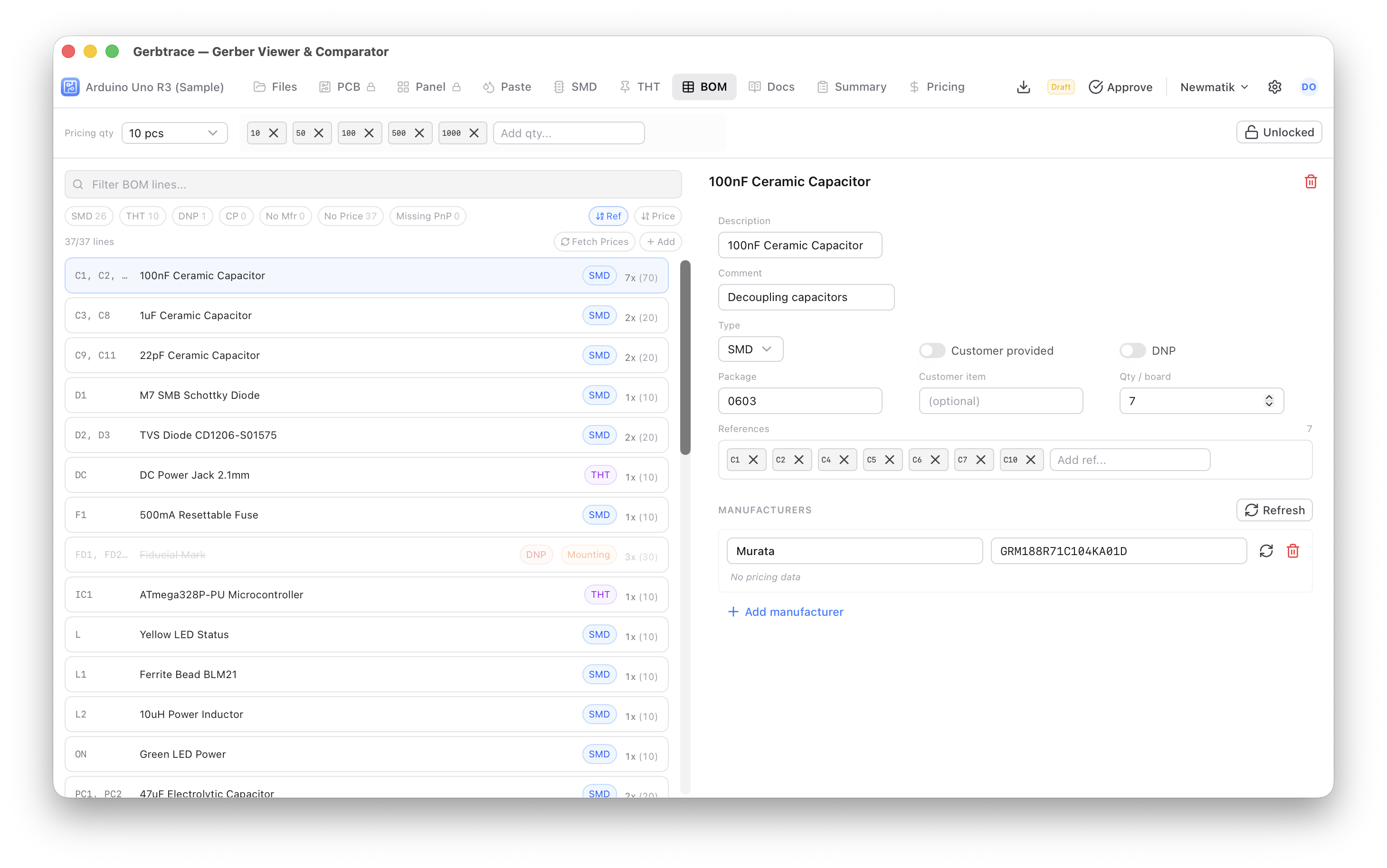
BOM Management

Import, enrich, and price your bill of materials

Import BOM files from Excel or CSV and organize components into custom groups. Automatic part matching suggests standardized descriptions and manufacturer part numbers. Add multiple manufacturers per component and fetch live pricing from global distributors.

  • Import from Excel, CSV, or manual entry
  • AI-powered part enrichment with Spark AI
  • Multiple manufacturers per component
  • Live distributor pricing with quantity tiers
  • Cross-reference with pick and place data
  • Filter by SMD, THT, DNP, or missing data
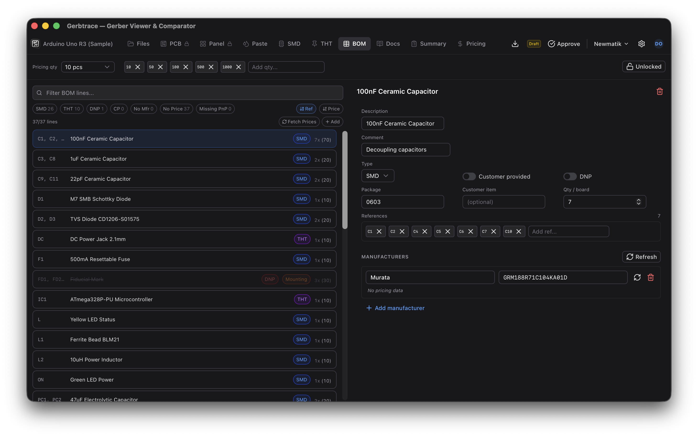
BOM management panel with component groups and pricing

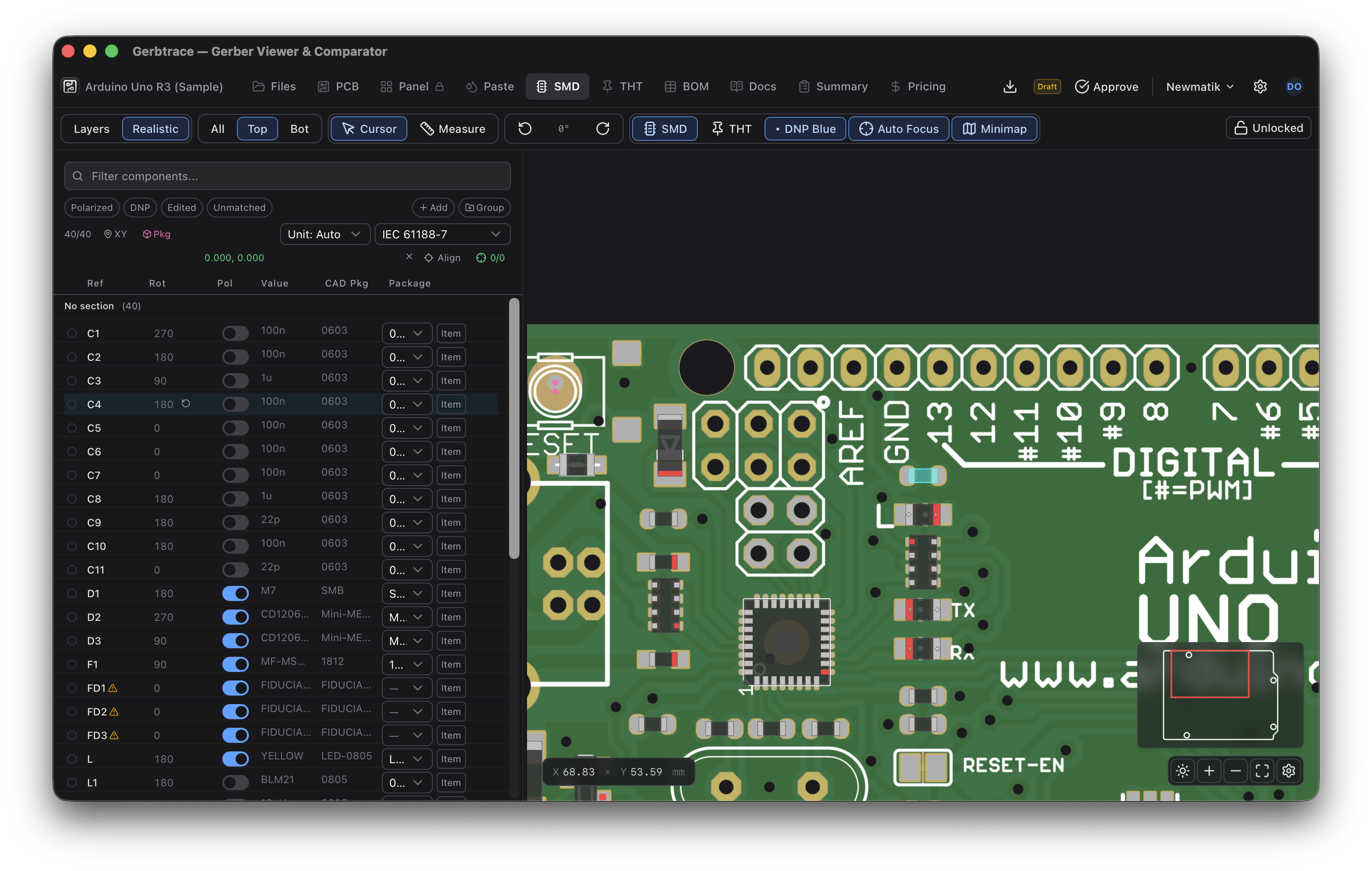
Pick and Place

Verify component placement and export machine files

Visualize SMD components directly on the PCB canvas with bidirectional highlighting. Match CAD package names to library packages, edit rotations, and verify polarity. Support for Mycronic, IPC-7351, and IEC 61188-7 rotation conventions.

  • Visual component placement on PCB canvas
  • Automatic CAD-to-library package matching
  • Multiple rotation convention support
  • Polarity and orientation verification
  • Batch editing and group operations
  • Export production-ready placement data
Pick and place visualization with component highlighting on PCB

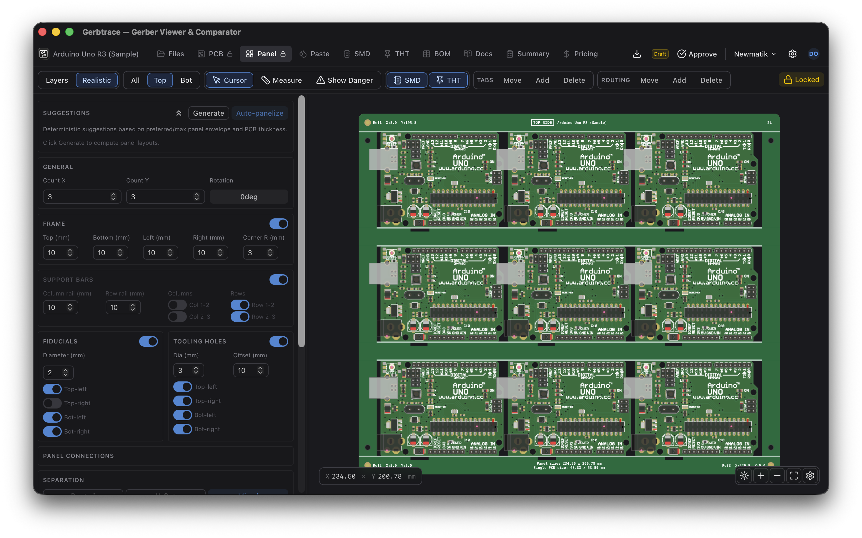
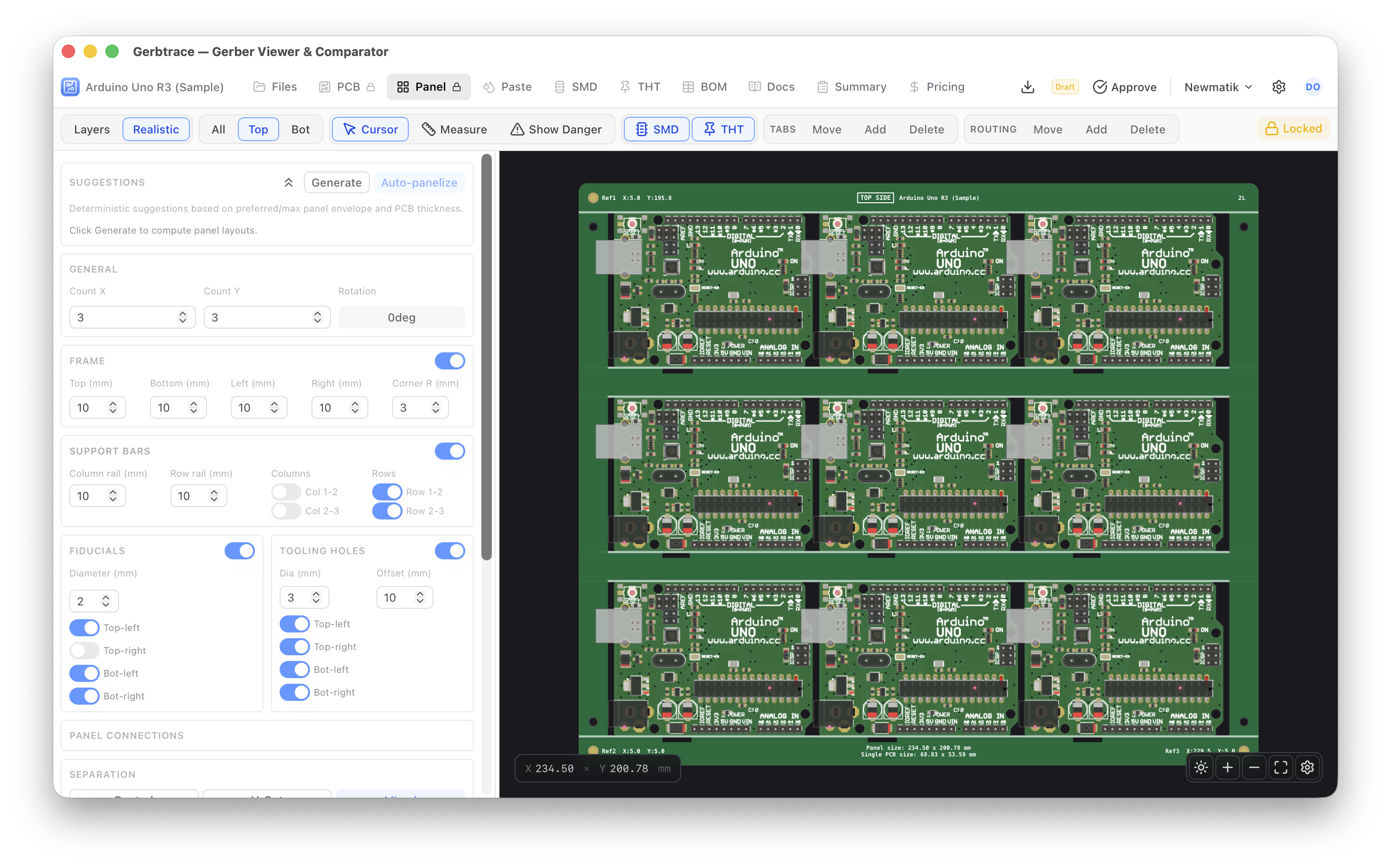
Panelization

Create production panels with frames and tooling

Configure multi-up panel layouts with grid settings, frame rails, fiducials, and tooling holes. AI-powered suggestions optimize board count within your panel size limits. Choose between routed channels with breakaway tabs, V-cut, or mixed separation.

  • Grid layout with AI-optimized board count
  • Frame rails, fiducials, and tooling holes
  • V-cut, routed tabs, or mixed separation
  • Mouse bite perforation configuration
  • Support bars between columns and rows
  • Real-time canvas preview with components
Panel configuration with grid layout and frame settings

Paste and Stencil

Configure solder paste for stencil or jet printing

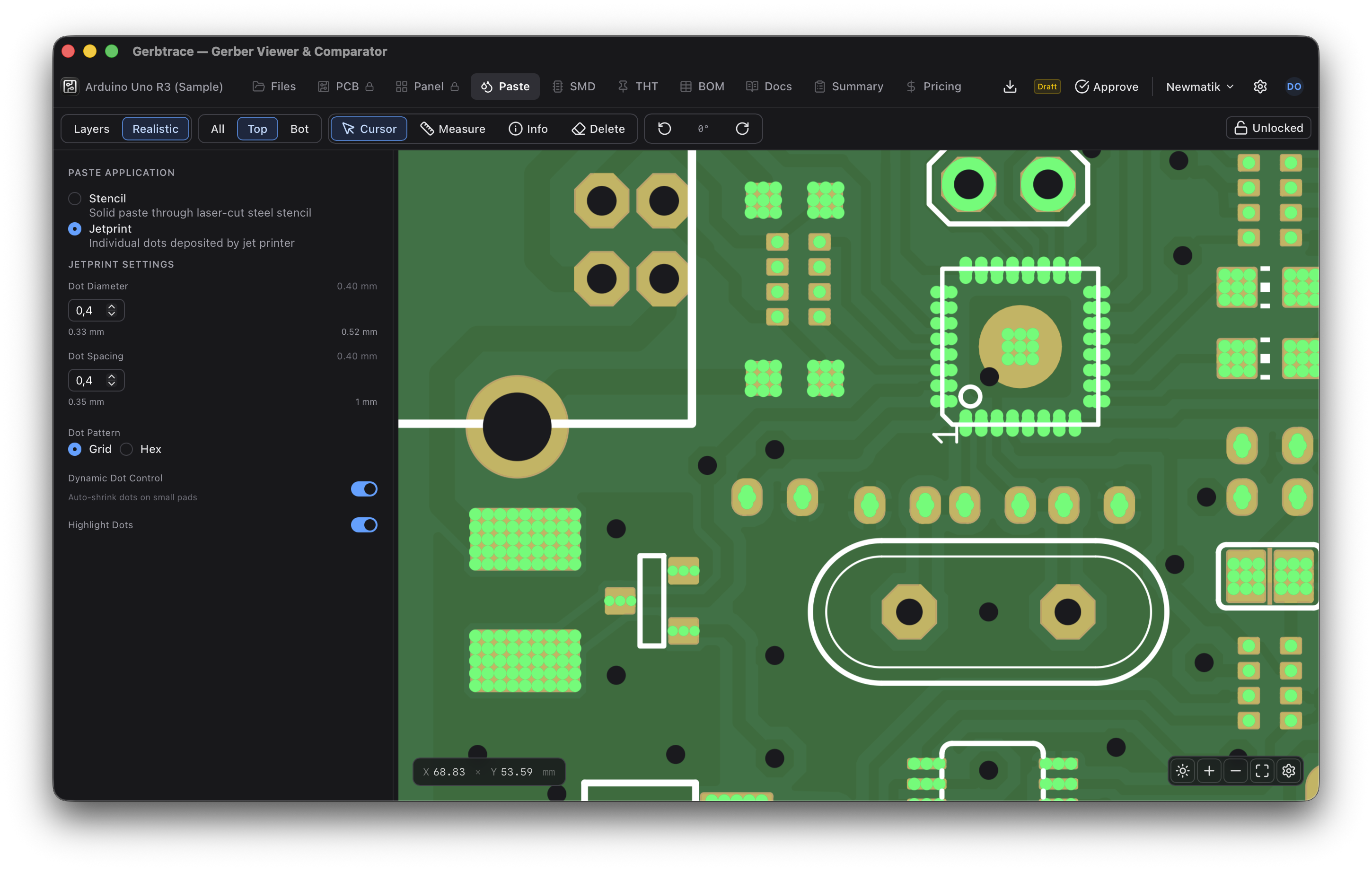
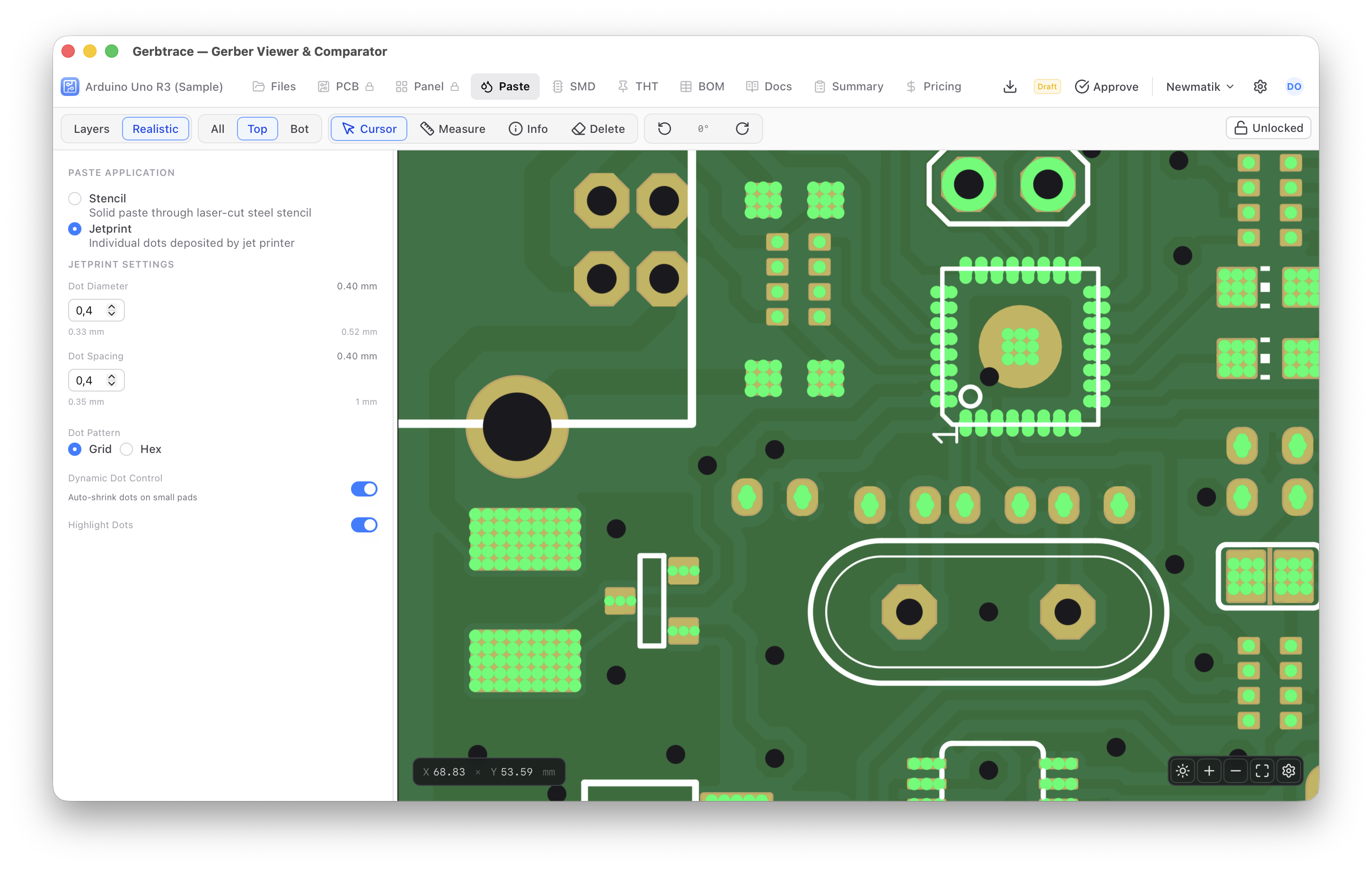
Set up solder paste for traditional laser-cut stencils or stencil-free jet printing. For jet printing, configure dot diameter, spacing, and pattern for each pad. Compatible with Mycronic MY600 jet printers with direct JPSys JSON export.

  • Laser-cut stencil configuration
  • Jet printing mode (Mycronic MY600)
  • Adjustable dot diameter and spacing
  • Grid or hexagonal dot patterns
  • Dynamic dot control for small pads
  • JPSys program export
Solder paste jet printing configuration

Production Summary

Assembly overview and manufacturing handover

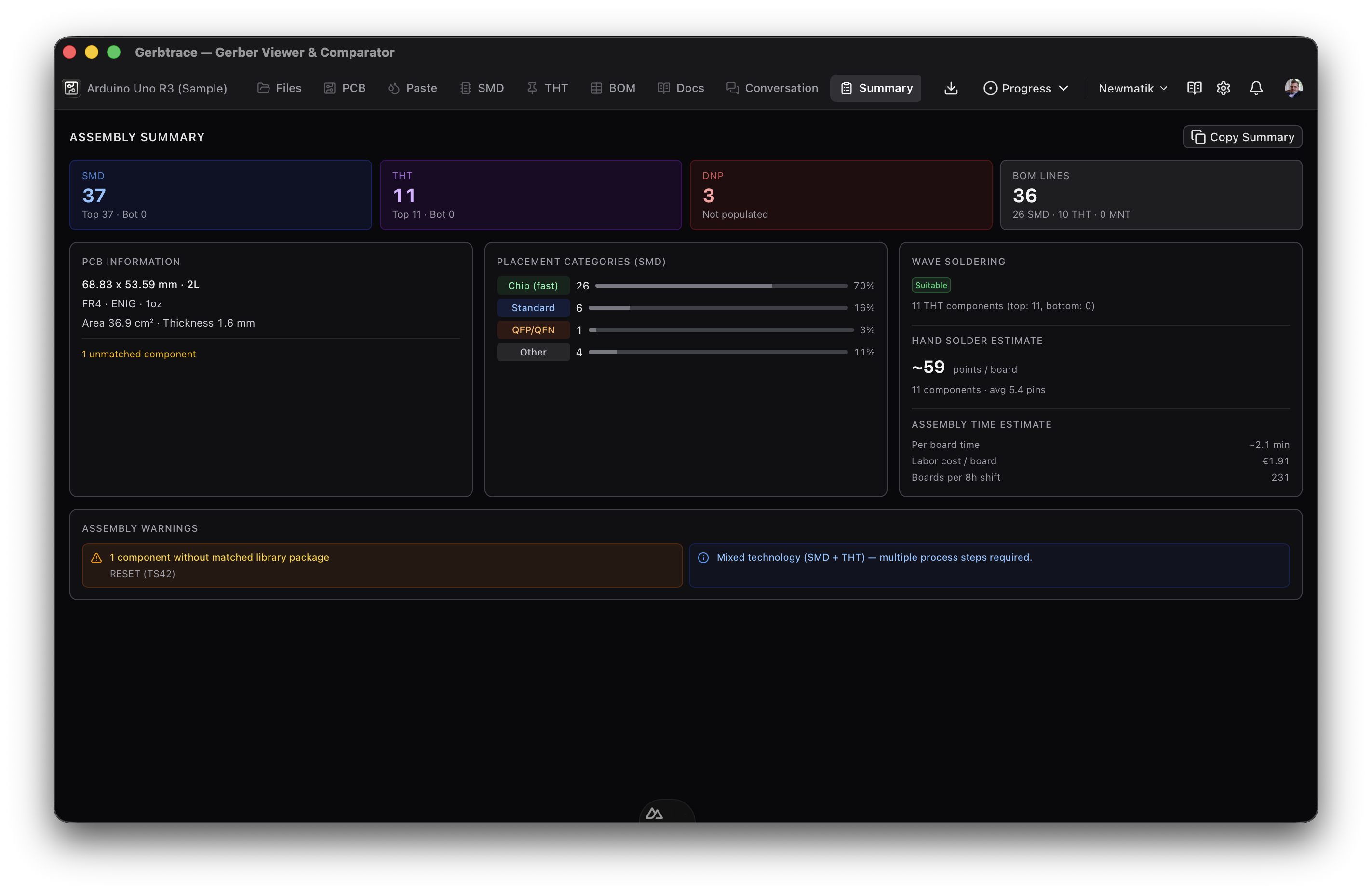
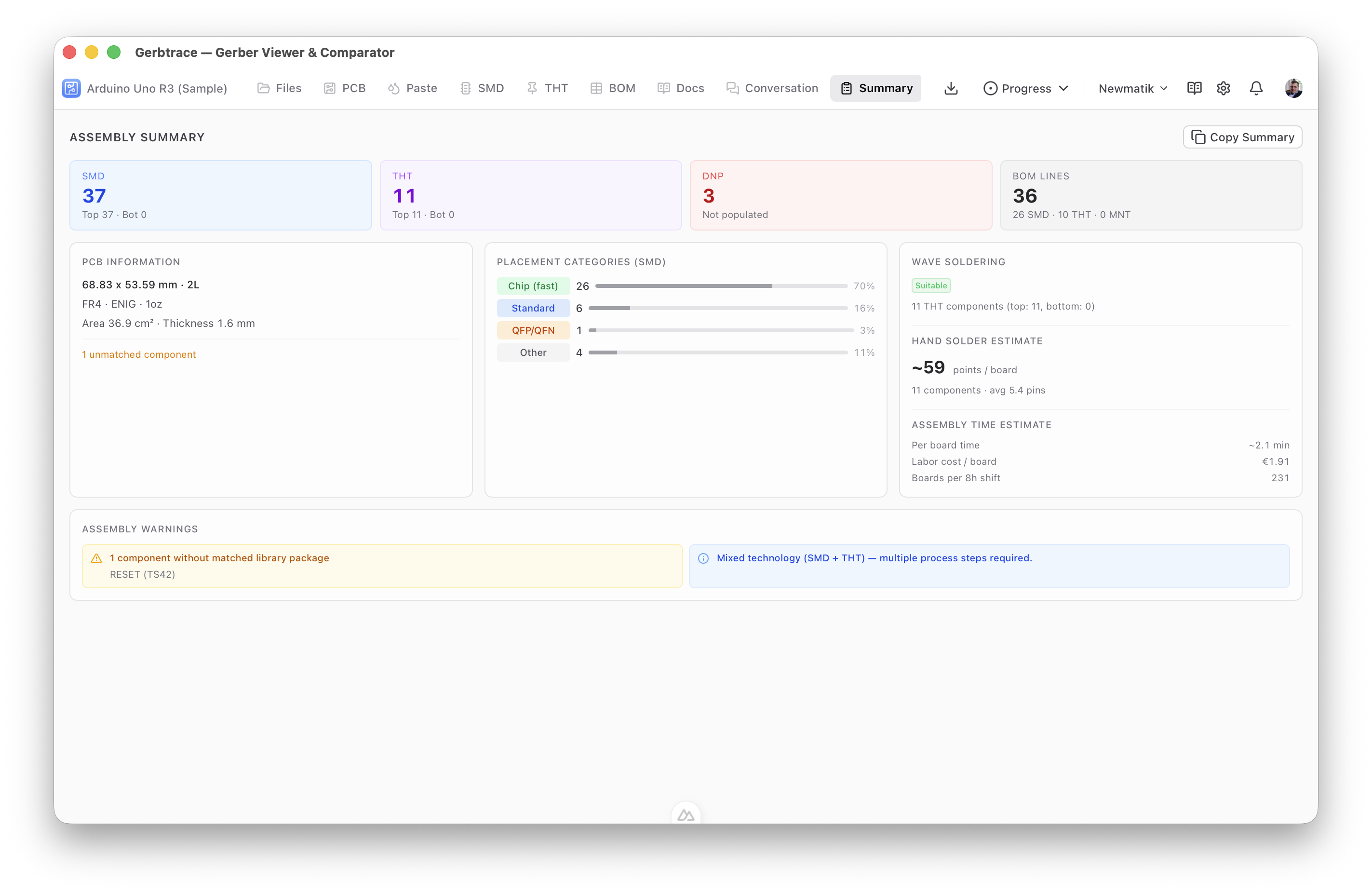
Get a complete assembly overview with component counts broken down by SMD and THT, placement speed categories, wave soldering suitability, and hand solder estimates. Assembly warnings flag production considerations like BGA, fine-pitch, or mixed technology boards.

  • Component count breakdown (SMD/THT by side)
  • Placement speed categories (chip, standard, QFP)
  • Wave soldering suitability check
  • Assembly warnings for production
  • Cost estimation with quantity tiers
  • Copy summary to clipboard for quotations
Production summary with assembly overview and cost estimation

From design files to factory floor

Step 1
Import

Drop Gerber, BOM, and PnP files

Step 2
Review

Inspect layers, verify components

Step 3
Prepare

Panelize, configure paste, enrich BOM

Step 4
Price

Get live component and assembly costs

Step 5
Hand Off

Export production-ready data

Start preparing your PCB data

Free to start. All NPI tools are available on every plan.